Can I define regions of different mesh sizes inside a polygon in CST MWS?
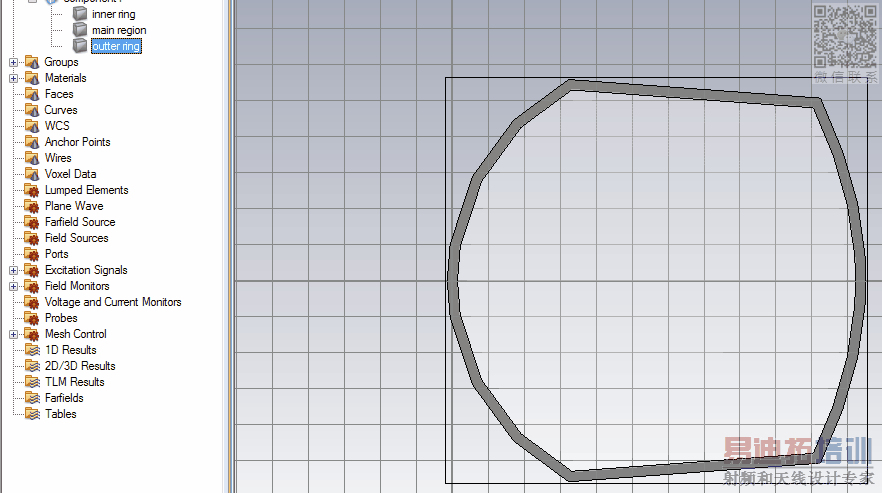
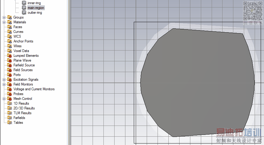
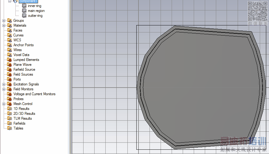
Hello everyone. I have an electrically very large polygon and innevitably the generated mesh is very large wich leads to impractical large simulation time. What i did was to seperate the polygon in 3 rings so i created first an outter ring and defined a local fine mesh(lamda/10) then i created the second ring and defined a more coarse mesh(lamda/6) and defined the rest of the region as a polygon of mesh cell size lamda/4. But the thing is that when i merge the 3 parts to perform the simulation the created component keeps the local mesh properties of the middle ring. Is there any way to make regions on the same polygon consisting of different mesh cell sizes? To be more specific, i also attached some image of the structure.
Thank you!


If you unite the geometries, the mesh definitions will be combined also. If you want to have different mesh densities for different parts, you must keep them separate. This will work fine for frequency domain and integral equation but it is more complicated for time domain.
Are you using time domain solver? Are you using TLM meshing? Unless you use TLM meshing, the inner component will be meshed as finely as the outer mesh. I think TLM allows for irregular mesh, but Im not sure. If the object is PEC, it is likely that CST already knows this and skips the calculation for the interior already.
Hi Nhera,
Yes i'm using the time domain solver which takes huge amounts of time for simulation.I used hexagonal mesh(not tlm). I used the integral solver once but i cannot simulate my structure for a frequency band, but for a single frequency. If the different meshing is possible in frequency domain solver as you mentioned i will try to do it there. Also the polygon structure attached above is PEC. Thank you.
Is the object 3D? You dont need any meshing for the interior of the PEC at all. I think CST skips the calculation for the interior of the object anyway, so there is no point in defining a coarser mesh.
What kind of problem is this? What is the size of the object in wavelengths? What is the band of interest?
the object is a microstrip cavity and under the cavity a very thin substrate will be placed(height=0.1 mm) so it is a planar structure. I used subgridding when used the transient solver so the interior will be meshed coarsely but the mesh was pretty large even with that option. The size of the object is 40*lamdax40 lamda so it is a very large electrically structure. What i want to do is to draw some lines wich will expand outwards of the structure (say 1 lamda) at both sides of the structure so i can put ports at the lines and simulate the object to get the s parameters. The band of interest is from 27 GHz to 33 GHz.
You can apply individual mesh properties to any object in project, just right-mouse-click on object in project-tree and select 'Local mesh properties'. But i think that Your problem is not in this, looks like a problem with specific analyze of electrically large structures. If You upload Your *.cst file i can help You more.


